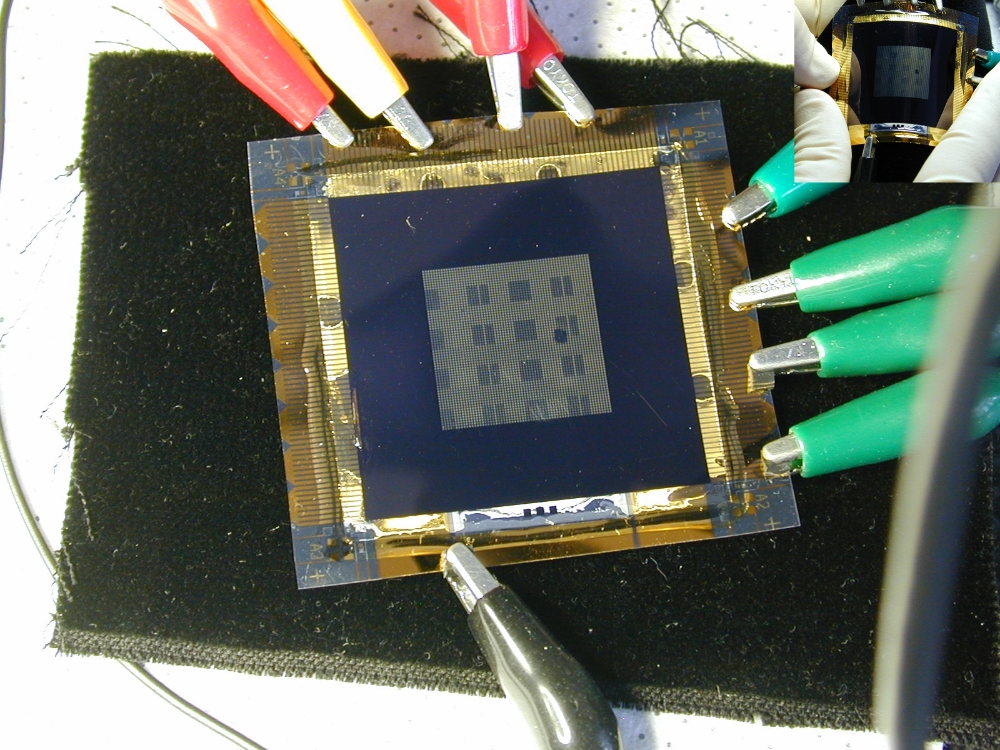
Thin Film Transistors, Circuits, and Backplanes
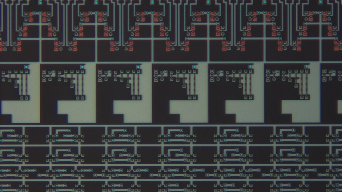
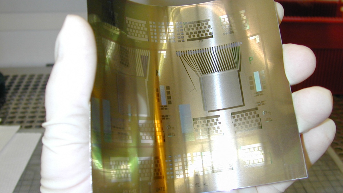
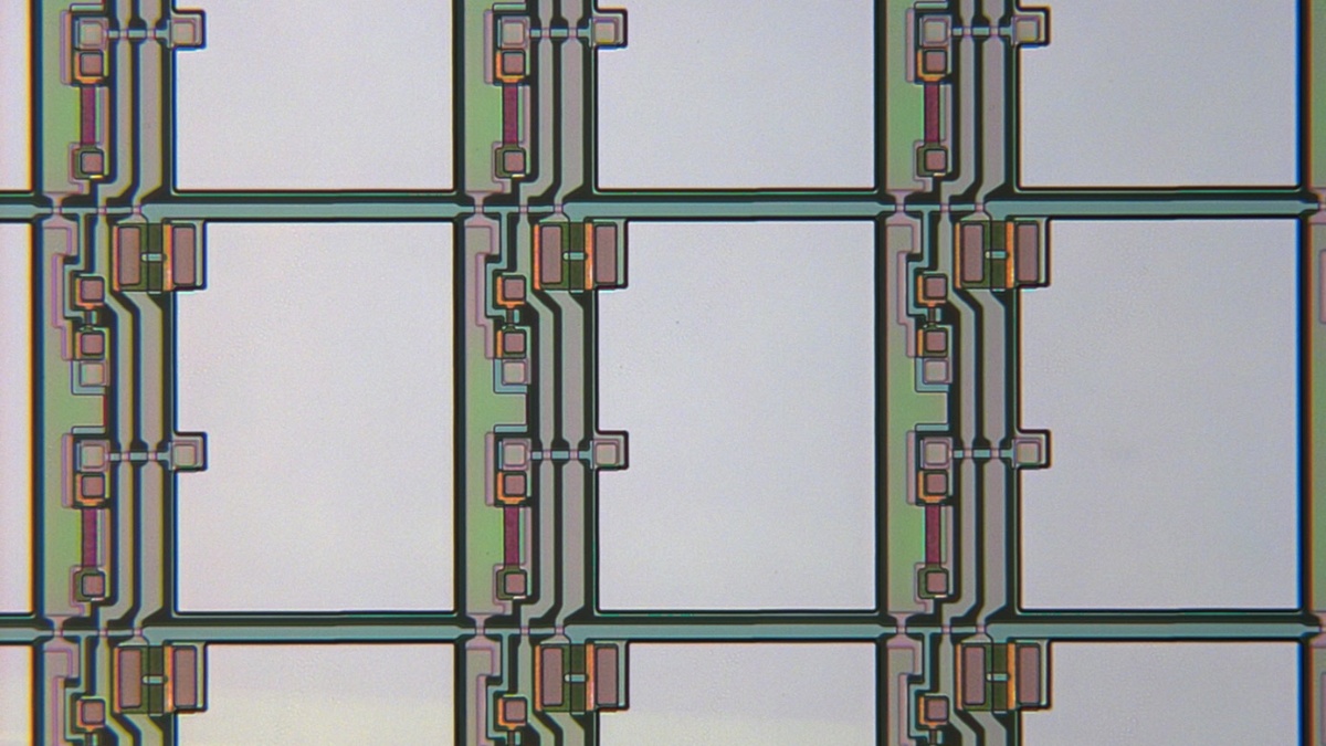
The IGM and its predecessor organizations have been investigating thin film transistors (TFTs) for integration of electronics on non-mono-crystalline surface (glass, plastic foil, metal foil) since the late 1970s. The trasistors are processed at the in-house clean room opened in 1993. All processes relevant to TFT or flat panel production can be performed on substrates of up to 16 inches squared. The clean room provides the IGM with the capabilty of researching new and improved processes for the production of TFTs as well as more complex systems such as integrated circuits (shifting registers, logic, operation amplifiers) and active matrix backplanes for LCD and OLED flat panel displays.
The IGM can process substrates up to 16 inches squared.
Currently the IGM can implement the following TFT technologies
Field effect transistors based on amorphous silicon are the foundation of flat panel technologies. They can be processed at moderate temperatures (<300°C) using plasma enhanced chemical vapour deposition (PECVD). Just like crystalline silicon, silicon atoms in amorphous silicon have a valence of 4. They do not, however, form a symmetric lattice but a far less regular structure with widely varying bonding lengths and angles. Open bonds are saturated with hydrogen. The resulting solid-state material results in a limited mobility for electrons and virtually no mobility for electron holes. Maximum carrier mobility is limited to below 1cm²/Vs beschränkt (for comparison, mono-crystalline silicon offers a carrier mobility of about 500cm²/Vs). The corresponding speed of a-Si:H based circuits is limited to a few hundred kHz. One typical application for a-Si:H TFTs are the active matrices in computer displays and LCD tvs.
s-Si:H TFTs have a number of advantages as well, namely small reverse-leakage currents with correspondingly high switching ratios, low cost and good industrial availability.
Both bottom-gate (industrial standard process) and top-gate (process developed at the IGM to reduce complexity) TFTs can be processed at the IGM.

Polycrystalline low temperature silicon (process temperatures limited to below <500°C) is created by exposing a thin layer of amorphous silicon (50nm) to a high energy pulse from a uv-laser, melting the silicon. In the process, the uv radiation will be absorbed in the silicon layer without heating the (far thicker) glass substrate underneath. As the molten layer of silicon cools, it forms crystals starting from random crystallization seeds. The result are single, small, high quality silicon crystals of typically a few 100nm size surrounded undesired grain boundaries.
The high quality increases the carrier mobility compared to a-Si:H drastically, up to about 100cm²/Vs for electrons and about 50cm²/Vs for electron holes. This increases the operating speed up to 100 MHz, allowing the implementation not only of the active matrix but also of far more complex control circuits (eg driver circuits) that can now be integrated directly on the substrate.
These advantages of LTPS are somewhat mitigated by an increase in processing complexity compared to a-Si:H.
The increased carrier mobility allows for the design of smaller transistors, making LTPS a popular technological choice in smartphones, tablets, and high resolution notebook displays.
Currently, the IGM can implement NMOS, PMOS, and CMOS LTPS-processes.

Indium-Gallium-Zinc-Oxide is a comparatively new material that is only being investigated as a candidate for thin film semiconductor applications since the early 2000s. IGZO can be sputtered at room temperature or used for printing in appropriate inks, avoiding the necessity for vacuum technology. Even though IGZO form amorphous layers, its electron mobility is better than most amorphous semiconductors at about 10cm²/Vs to 20cm²/Vs. The mobility of electron holes is a lot lower. The large band gap makes IGZO optically transparent, making it a good match of transparent electronics in displays or smart glass. IGZO layers can be processed at room temperature, but good quality transistors require processing steps at temperatures of about 300°C.
IGZO is best suited for application where a-Si:H is not fast enough, but very high speeds and integrated CMOS-circuits are not required.
The IGM can process IGZO on both glass and plastic foils.
Organic semiconductors include a whole class of different materials. They all have an organic, ie carbon molecule based, chemistry in common. These molecules can consist of some ten or hundreds of atoms (small molecules) or millions of carbon-based submolecules (polymers). All organic semiconductors offer relatively good conductivity for electrons within the molecule with comparatively high energy barriers between molecules. The resulting carrier mobility is about 1cm²/Vs to 5cm²/Vs, but can be several orders of magnitude lower for many of the organic semiconductors. Generally speaking, small molecule materials have better electric properties while polymers are easier to process. Both N and p type transistors are possible, although p-type OTFTs tend to be of better quality.
Organic semi conductors can be processed at comparatively low temperature, ranging from room temperature to about 100°C, making them well suited for processing on plastic foil sustrate.
Currently the IGM is capable of processing OTFTs both from CVD or from printing.

Carbo nano tubes (CNT) are tubes of a few nanometers in diameter and a few micrometers in length that consist of "rolled up" single layers of graphene. Depending on the angle between the symmetry of the graphene and the "rolling" process (chirality) CNTs can show metallic (good conductivity) or semi-conductor behavior.
Carrier mobility within a single CNT can be very high (up to 100000cm²/Vs). Unfortunately, current process technology does not allow for the precise placement and orientation of a large number of CNTs on a substrate, only random networks of CNTs are possible. The resulting carrier mobility is correspondingly lower, about 1cm²/Vs to 10cm²/Vs. These values can, however, be expected to increase drastically as the technology matures.
Another application for CNT would be metallic, transparent layers of CNTs for pixel electrodes in LCDs.
Currently, the IGM can process CNT-TFTs as well as LC cells and OLEDs with CNT electrodes.
Further Information
Holger Baur
Dipl.-Ing.Deputy Head of Institute, Head of department
Patrick Schalberger
Dr.-Ing.Deputy Head of Institute, Head of Laboratory