Current Topics/Projects
You will find a current list of all projects in ILIAS (you will have to join the ILIAS group)
Can't find anything that interests you?
Please ask for more ideas
Our research and development activities always uncover new topics, new avenues of investigation, new ideas that can be used to define a graduate or research thesis. You will find a short list of fields of research below. Please contact us if you are interested in any of those topics.
...or contact us with your ideas
You are looking for a supervisor for your own concrete idea for a thesis? Just contact us.
Fields of Research
Silicon is the classic semi conducting material for thin film transistors (TFTs). The IGM can process TFTs based on amorphous, microcrystalline, or laser-crystallized poly-crystalline silicon. While amorphous silicion is well suited for large area processing (in tv substrates of up to 10m2), poly-crystalline silicon offers far better (up to a factor of 100) carrier mobility and the option of processing complex CMOS circuits directly on glass.
Projects in this field include
- Simulation and design of poly-crystalline silicon circuits
- Processing of thin film elements and circuits
- Electronic characterization of processed elements
- Optimization of thin film processing techniques
- Processing of active matrices in poly-crystalline silicon
Contact:
Thin film transistors (TFTs) are the basic elements for integrated circuits used in LCD or LED/LCD flat panel displays (computer monitors, tvs, tablets, and smartphones). Current developments aim at replacing the dominant LCD technologies with active matrix OLED (AMOLED) technologies. At the moment, AMOLED displays for mobile devices are implements using comparatively costly poly-crystalline silicon transistors. Metal-oxide semiconductors like Indium-Gallium-Zinc-Oxide (IGZO) can offer a cheaper alternative as the semi-conductor in TFTs. In addition, combining IGZO with OLEDs would allow the production of completely transparent displays.The IGM offers the capabilities to develop and realize large area transparent integrated thin film circuits from the simulation to the pruduction of photo lithographic masks to the final processing.
Projects in this field:
- Design and simulation of integrated circuits
- Processing of thin film elements and circuits
- Electronic characterization of processed elements
- Optimization of Gatedielectrics
- Stability Testing
- Optimization of the thin film processing techniques used
- Processing of active matrices using metal-oxide semiconductors
- Processing of integrated circuits on flexible substrates
Contact:
Projects in this field:
- Building LC cells for different types of liquid crystals
- Optical characterization of cells
- Development of color filters
- Optimization of the thin film processing techniques used
Contact:
Research has resulted in the creation of powerful organic materials that have already found their way into commercial products as semiconductors in field effect transistors (OTFT) or in light emitting diodes (OLED).
Projects in this field:
- Optimization of the thin film processing techniques involved in the processing of OTFTs
- Testing of alternative dielectric or semiconducting organic materials for use in OTFTs
- Electric and optic characterization of the elements and layers processed.
Contact:
Metrology at the IGM focuses on the determination of the physical properties of thin films and liquid crystal cells. It serves to evaluate and to improve current processing techniques. The IGM features a variety of instruments and techniques to characterize for example thin film transistors and thin film capacities.
Projects in this field:
- Setting up or expanding existing metrology systems
- Programming of automated measurement processes
- Adaptation of a measurement robot for additional automated measurement processes
Contact:
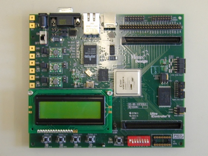
Control and address circuits form the interface between a display (e.g. AM-LCD) and the graphics or video signal. They can be separated into the driver circuits for addressing the actual pixels, attached directly to the screen, and the interface adapting the input signal to address those driver chips.
Projects in this field:
- Testing of drivers and signal sources
- Programming (e.g. FPGAs in VHDL)
- Circuit design
- Simulation
Contact:
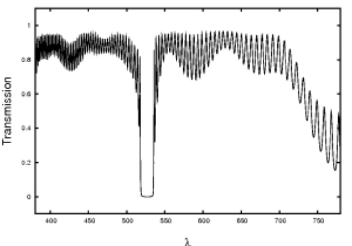
Shifting the processing of signals from electronics to optical systems can help improve the efficiency pf optical signal transfers. Optical signal processing can be realized in a variety of ways, from well-established interference filters to using active components loaned from display technologies.
Projects in this field:
- Design and synthesis of optical thin film filters
- Design of numerical methods for the synthesis and analysis of optical filters
- Programming of algorithms for the synthesis and analysis of optical filters (Maple, MATLAB, C/C++)
- Processing of optical thin film filters
Contact:
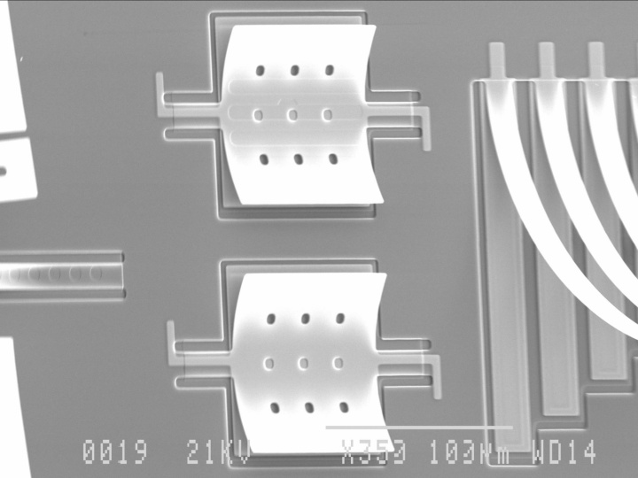
The IGM is researching the adaptation of established flat panel processing techniques to build large area micro electro mechanical systems. Possible applications include ultra-sonic transducers, MEMS displays, sensors, energy harvesting.
Projects in this field:
- Design and realization of MEMS-Elements
- Development of new processing techniques
- Simulation of micro mechanical structures (COMSOL)
- Integration of micro mechanical elements in thin film technology
Contact:
Further Information:

Patrick Schalberger
Dr.-Ing.Deputy Head of Institute, Head of Laboratory

Annika Schmekal
M.Sc.Scientific staff member


