Equipment
The Clean Room
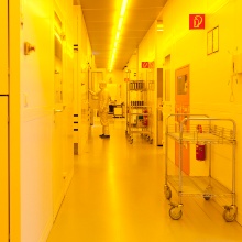
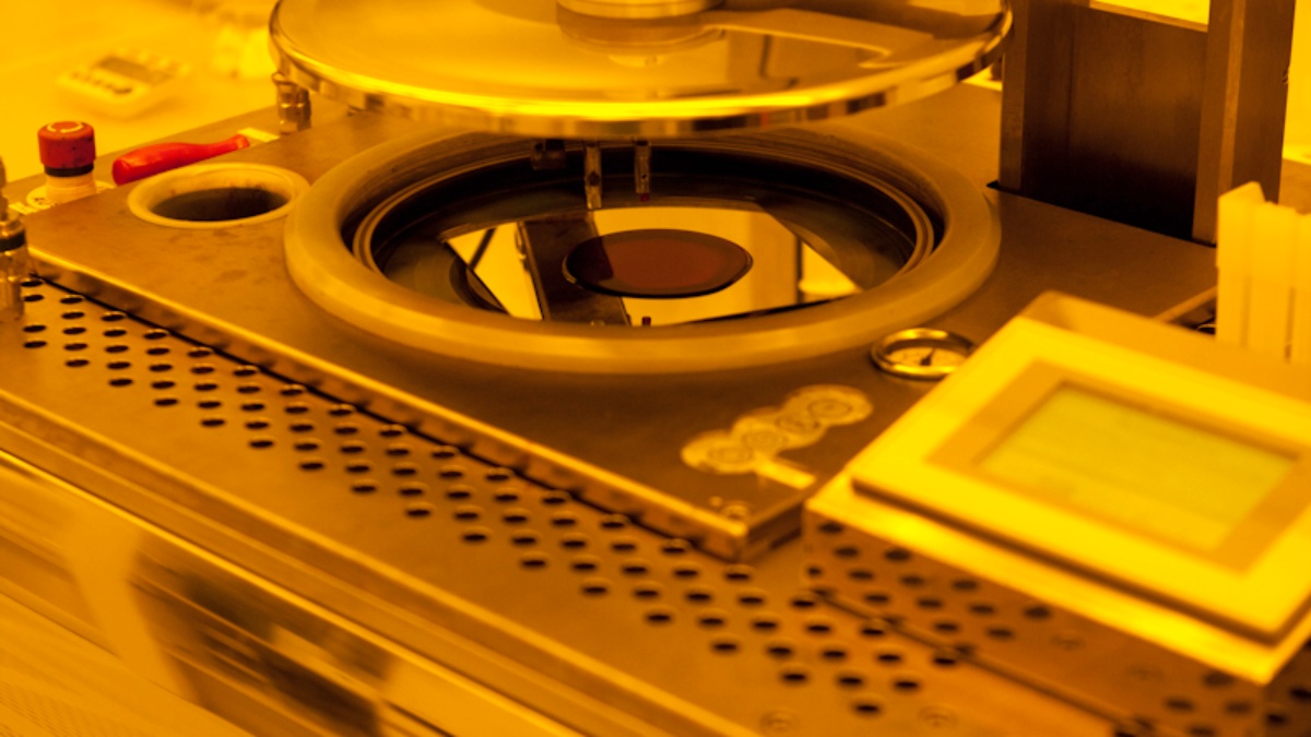
The facilities at the IGM include more than 500m2 clean room. The majority of that area or about 480m2 are the main lab with a very high purity class for a research fertility (ISO5, less than 100 particles with a size of more than 0,5μm per cubic foot of air; ISO 4, less than 10 particles with a size of more than 0,5μm per cubic foot of air, in the area with the lithographic devices). The IGM is fully equipped to produce flat screens and similar thin film devices in near-industrial processes. The close similarity of the equipment and processes to industrial facility supports the technology transfer to industrial production lines.
A second, smaller clean room contains 3 MBraun glove boxes with a nitrogen inert atmosphere for the processing of organic semiconductors which are very sensitive to oxygen and humidity.
The following devices and facilities are available at the IGM:
- PECVD:The IGM features several PECVD reactors, including one Balzers (Oerlikon) KAI 1M reactor for the deposition of amorphous or polycrystalline silicon (including doping), silicon nitrate, and silicon oxide on glass substrates up to 16 inches squared.
- Sputtering: Two Leybold ZV6000 inline-sputtering systems equipped with a total of 12 different targets (9 DC and 3 RF) are available at the IGM. Targets for typical display materials like chromium, aluminium, molydaenium but also gold, nickel, palladium, ITO, AZO, IGZO are available. Numerous additional targets can be mounted as necessary. The sputter system can handle substrates of up to 16 inches squared. The first ZV6000 sputtering-system had been fundamentally refurbished in 2017. In 2020, together with the company HS-Group GmbH, we had been able to perform the modernization of the second sputtering-system as well. Now, both systems are state-of-the-art regarding to PLC system control, user interface, gasflow control, pressure measurement/-control and substrate transport drive. This enables new possibilities for deposition process optimization and allows for a long term perspective of operating the machines.
- Vapor Deposition: The IGM offers access to a Lesker Spectros vapor deposition system with two separate sources for metallic material and eight sources for organic material. The system is integrated into the inert-gas glove boxes to enable oxygen and moisture free handling of OTFTs and OLEDs. In addition the IGM features two older Balzers systems with thermal and electron beam vaporization systems. All vapor deposition systems can handle substrates of up to 6 inches squared.
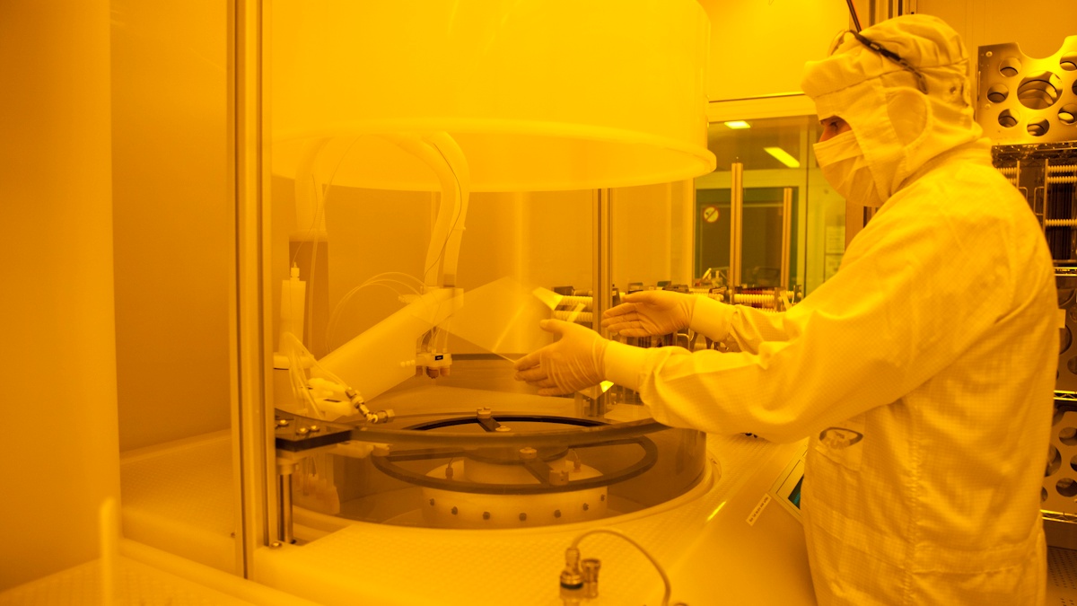
- Spin Coating: The IGM operates several spin coaters for the deposition of photo resist and other liquids onto substrates of up to 16 inch squared. One smaller spin coater for substrates of up to 6 inches squared is integrated into the inert-gas glove boxes.
- Printing: Several printers for the direct deposition of structured layers are accessible at the IGM. Screen printers allow the large area deposition of material at a high volume but require a specifically made screen as a mask. A Dimatix inkjet printer can deposit almost any solution or suspension without the need for a complex physical mask.
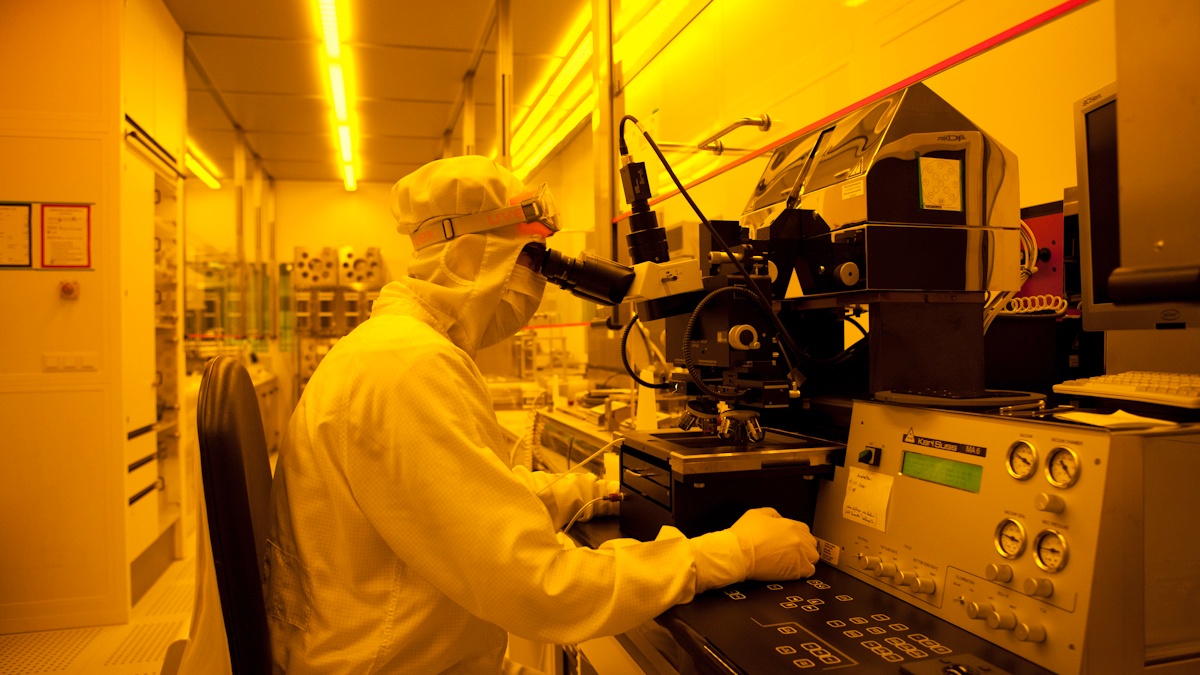
- Lithography with Photo Masks:The IGM is equipped with two contact exposure systems of type Süss MA6 for processing substrates of up to 6 inches squared. This allows for the realization of structures down to 3 µm.
- Direct Imaging:The IGM features a Heidelberg Instruments DWL 400 direct imaging system that can realize structures down to 2μm on 16 inch squared substrates without requiring complex photo masks.
- Ion Implantation: Access to an ion implantor type Eaton (Axcelis) NV3206 is offered at the IGM. The standard airlock has been replaced with a larger one allowing the processing of substrates up to 16 inches squared. The system can implant phosphorus, boron, fluor, and argon ions at up to 200kV.
- Excimer-Laser: A Sopra VEL Excimer Laser for the recrystallization of amorphous into polycrystalline silicon is available at the IGM. The XeCl laser operates at a wavelength of 308nm and can fire 200ns pulses of up to 15J each at a target area of 67mm by 27mm. It can also be used to activate doping or to improve the crystal quality of other semiconductors. The system can process substrates of up to 16 inches squared using stitching.
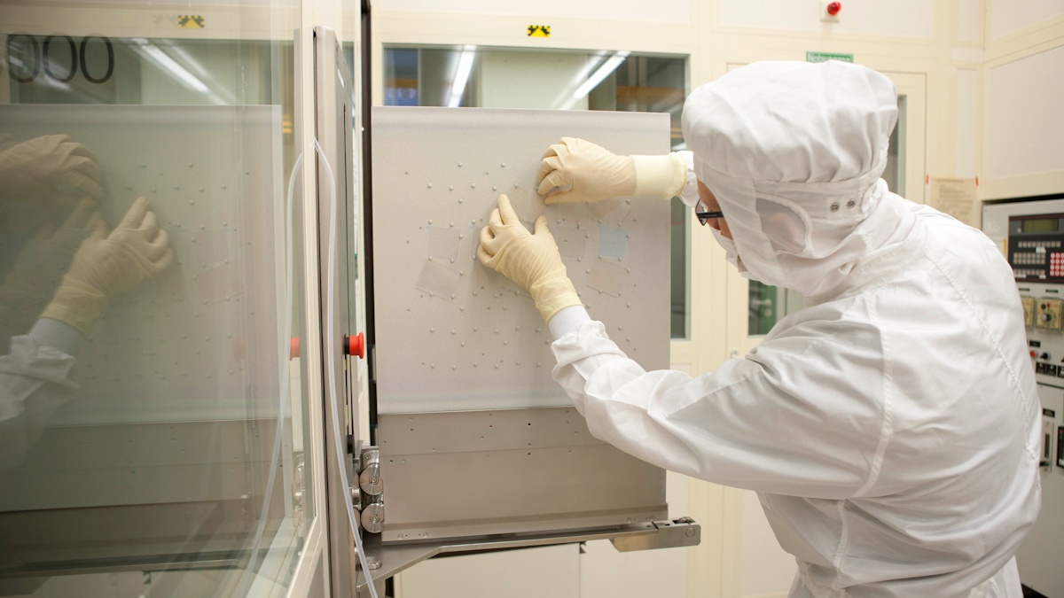
- UV-Ozone Treatment:The IGM features a UV-Ozone system to clean substrates or to improve surface adhesion. The combination of highly reactive ozone and high energy light can remove organic contaminants and can activate the surface by freeing chemical bonds in surface molecules. The system can process substrates of up to 16 inches squared.
- Rubbing:The IGM offers access a Hörnell Rubbing system to structure the polyimide orientation layer by rubbing with a velvet roll.
- Spacer Spray System: The IGM operates an electrostatic spacer spray system type Accudyne for 5μm spherical polymer spacer used to ensure a uniform thickness of the liquid crystal cell. Additional different sizes of spacers can be sprayed or spin coated.
- Glue Robot: A Schiller 3-axis (xyz) gantry robot is used to apply glue frames in the assembly of the two substrates into one liquid crystal cell.
- Filling Chamber: The IGM utilizes a dedicated Balzers vacuum chamber with a movable substrate holder to fill cells with liquid crystals.
- Cell Construction: The IGM featurs a wide array of additional tools supporting the micrometer alignment of sustrates.
All of the above systems can handle substrates of up to 16 inches squared.
- Waferprober: A Süss wafer prober in combination with a Keithley 4100 semi conductor measurement system allows for the reliable characterization of TFTs and other semiconductor electronic elements. Additional picoampere meters allow measurements in the cleanroom, in climate boxes and in intert-gas boxes.
- Viewing Angle Contrast Measuremen: An Eldim EZ Contrast 160 system is used for high-speed measurements of luminance, contrast and color space of transmissive and reflective or self-illuminating displays both in absolute values and their viewing angle dependency.
- Climate Chamber: A climate chamber allows for the controlled exposure to precisely definite environments, facilitating the evaluation of systems under different conditions and the simulated aging at increased environmental temperatures.
- Optical Microscopes: Several optical microscopes allow for quick inspections of processed substrates. Substrates of up to 16 inches squared can be checked.
- Scanning Electron Microscope: For inspections at resolutions above the limits of optical microscopes the IGM features a JEOL JSM 6400F SEM. This system has been modified for digital image generation.
- Atomic Force Microscope: The IGM features a DME AFM to determine surface topologies and surface roughness of layers.
- TAB Bonder: Several TAB (Tape Automated Bonding) devices, both manual and semi-automatic, are available for bonding Chips on foil (COF) driver chips onto glas substrates using anisotropically conductive adhesive film.
- Flip-Chip Bonder:unmounted silicon chips can be bonded upside-down (flip-chip) directly onto display glas. This technique saves space on the substrate and is therefore well suited to tablet and smartphone displays. The IGM operates a Süss flip-chip bonder.
Further Information
Holger Baur
Dipl.-Ing.Deputy Head of Institute, Head of department

Patrick Schalberger
Dr.-Ing.Deputy Head of Institute, Head of Laboratory


